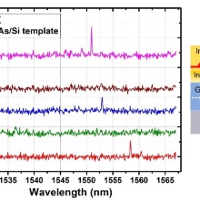
IPhotonic integrated circuits (PICs) based on the silicon-on-insulator platform currently allow high-density integration of optical and electro-optical components on the same chip. This high complexity is also transferred to quantum PICs, where non-linear processes are used for the generation of quantum light on the silicon chip. However, these intrinsically probabilistic light emission processes pose challenges to the ultimately achievable scalability. Here, an interesting solution would be employing on-demand sources of quantum light based on III–V platforms, which are nonetheless very complex to grow directly on silicon. In this paper, we show the integration of InAs quantum dots (QDs) on silicon via the growth on a wafer-bonded GaAs/Si template. To ensure emission in the telecom C-band (∼1550 nm), a metamorphic buffer layer approach is utilized. We show that the deposited single QDs show similar performance to their counterparts directly grown on the well-established GaAs platform. Our results demonstrate that on-demand telecom emitters can be directly and effectively integrated on silicon, without compromises on the performances of either the platforms.
Publication: Growth of telecom C-band In(Ga)As quantum dots for silicon quantum photonics
Ponraj Vijayan, Raphael Joos, Marco Werner, Jakob Hirlinger-Alexander, Matthias Seibold, Sergej Vollmer, Robert Sittig, Stephanie Bauer, Fiona Braun, Simone Luca Portalupi, Michael Jetter and Peter Michler![]() Mater. Quantum. Technol. 4
Mater. Quantum. Technol. 4
Contact person: p.vijayan
